Thermal Management Technologies

HIGH FREQUENCY DEVICES

Diamond Heat Sinks & Spreaders

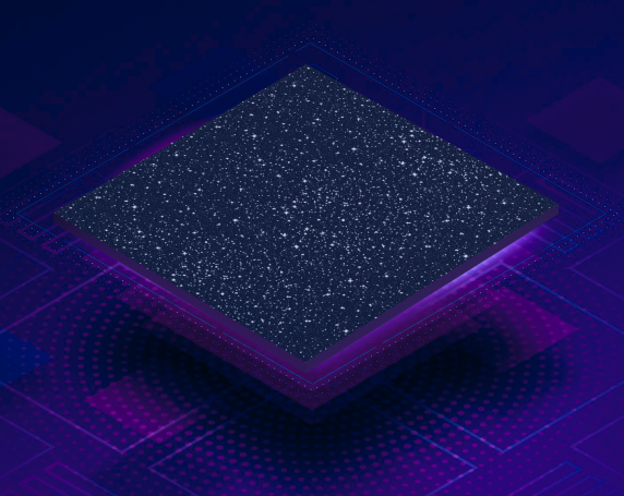
Diamond heat sinks set new standards in thermal management, enabling faster, more efficient, and more reliable electronics, ushering in a new chapter of technological advancement. Heat sinks are advanced thermal management components designed to dissipate heat efficiently from high-power and high-frequency electronic devices.

Karia Technologies is enabling essential technology for next-generation AI, quantum computing, power electronics, and high-performance communication systems at competitive prices, driving your technology and bottom line. Diamond’s exceptional thermal conductivity makes it an ideal material for heat sinks, significantly outperforming traditional materials such as copper and aluminum.

HIGH FREQUENCY DEVICES

Diamond Semiconductor Substrates

Karia Technologies empowers organizations to reach their technological advancement goals, with our Diamond Semiconductor Substrates and Diamond Wafers, enhancing the performance of electronic components, particularly in high-power and high-frequency applications. By using Diamond Semiconductor Substrates and Diamond Wafers as a component of semiconductor devices, we’re enabling advancements in AI power electronics, 5G/6G technologies, and quantum computing.

5G networks and the future 6G cellular technology will require high-frequency, high-power radio frequency (RF) devices for lightning-fast data transmission.

Industrial Devices

INDUSTRIAL DEVICES

Diamond Optical Windows

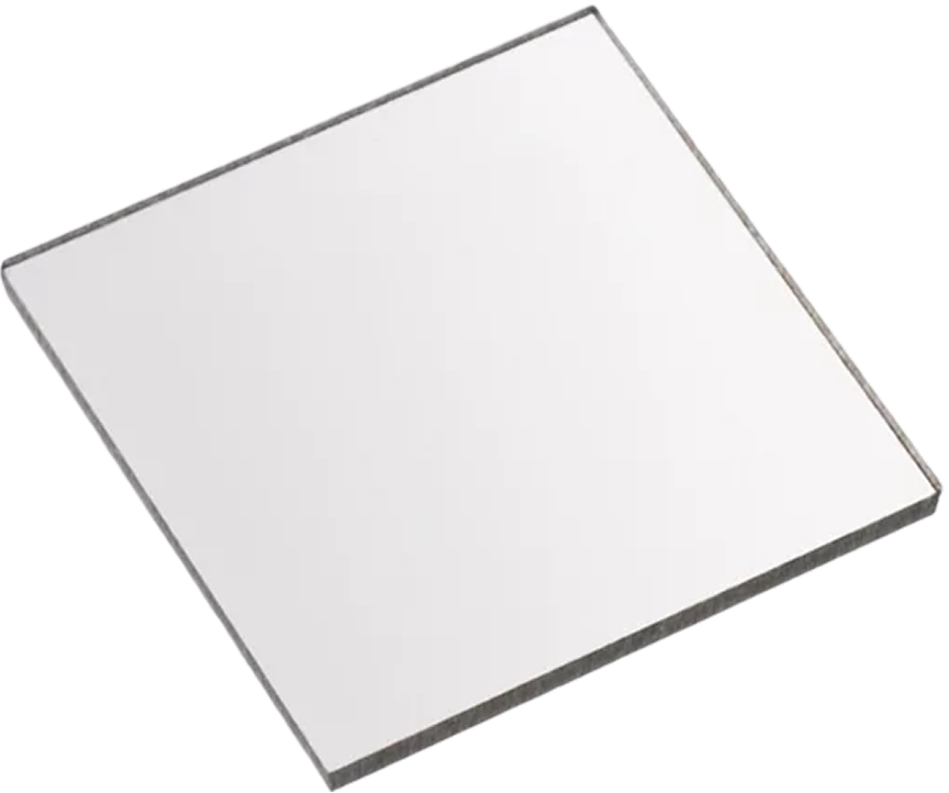
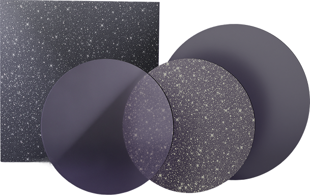
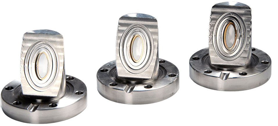
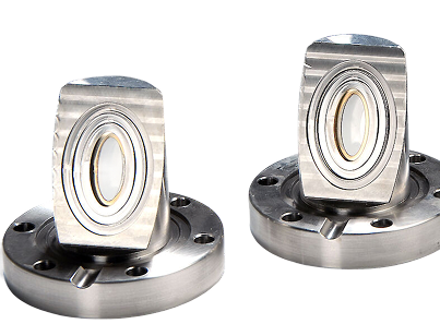
Karia offers a range of Diamond industrial products including Diamond Optics & Windows which are ultra-durable, high-performance transparent components used in extreme environments where conventional materials fail.

These windows provide superior optical clarity, thermal stability, and mechanical strength, making them ideal for advanced applications.

INDUSTRIAL DEVICES

Diamond Powders

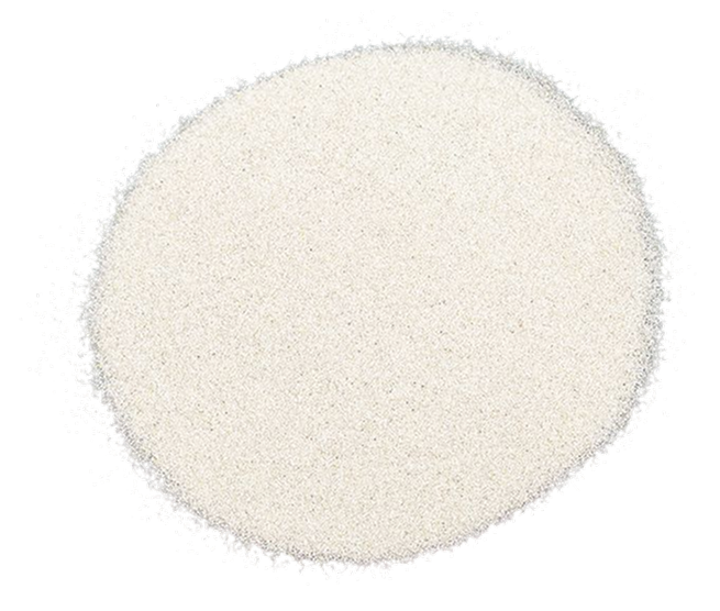
Karia Technologies also supplies its clients with Diamond powders which are finely ground, precision-engineered particles of diamond, produced from lab-grown diamond crystals.

Known for their extreme hardness, exceptional thermal conductivity, and chemical stability, diamond powders serve as the ideal abrasive and functional additive across diverse industries.

FEATURES

Outperform with Karia Solutions

Karia Offers a wide variety of products custom-built to meet your business needs and surpass your competition:

Single Crystal Diamond Wafers

Are ideal for ultra-high thermal conductivity, electronic performance, or quantum applications.

Polycrystalline Diamond Wafers

Are ideal if your technology needs large-scale thermal management, industrial durability, or cost-effective solutions—PCD wafers are more practical.

APPLICATIONS

Industry Applications

Power Electronics

Used in high-power transistors and diodes for energy-efficient systems.

RF and Microwave Devices

Enhances performance in telecommunications and radar applications.

Quantum Computing

Supports qubit development through nitrogen-vacancy (NV) centers in diamond.

Aerospace & Defense

Used in high-power transistors and diodes for energy-efficient systems.

Biomedical Sensors

Utilized in bioelectronics and implantable medical devices.

KEY PROPERTIES

Key Properties of Diamond Semiconductor Substrates (AI)

Feature Single-Crystal Diamond (SCD) Wafers Polycrystalline Diamond (PCD) Wafers
Crystal Structure Crystal Structure Composed of many small diamond grains with grain boundaries.
Thermal Conductivity Extremely high (~2200 W/m·K for pure SCD). Slightly lower (~1000–2000 W/m·K due to grain boundaries).
Electrical Properties Naturally an electrical insulator but can be doped for semiconductors. Typically an insulator, but grain boundaries can affect conductivity.
Mechanical Strength Higher purity and structural integrity. Slightly less strong due to grain boundaries.
Optical Transparency Extremely clear and transparent to a broad range of wavelengths. Less transparent due to grain boundaries causing light scattering.
Manufacturing Complexity Difficult and expensive to grow via CVD (Chemical Vapor Deposition). Easier and cheaper to produce, grown over a larger area.
Size Availability Limited to smaller sizes (~10–20 mm) due to growth constraints. Can be grown in larger wafer sizes (50 mm+).
Cost More expensive due to complex fabrication and purity. More cost-effective for large-scale applications.

GET A QUOTE

Ready to Get Started?

Whether you’re looking for a custom solution, product details, or just need pricing—our team is here to help.

We are excited to learn more about your project! So our team can best assist you, please select any of the boxes that best describe your project.

OTHER PRODUCTS

Explore Our Other Products

Diamond Heat Sinks

Diamond Optical Windows

Diamond Powders

Scroll to Top