

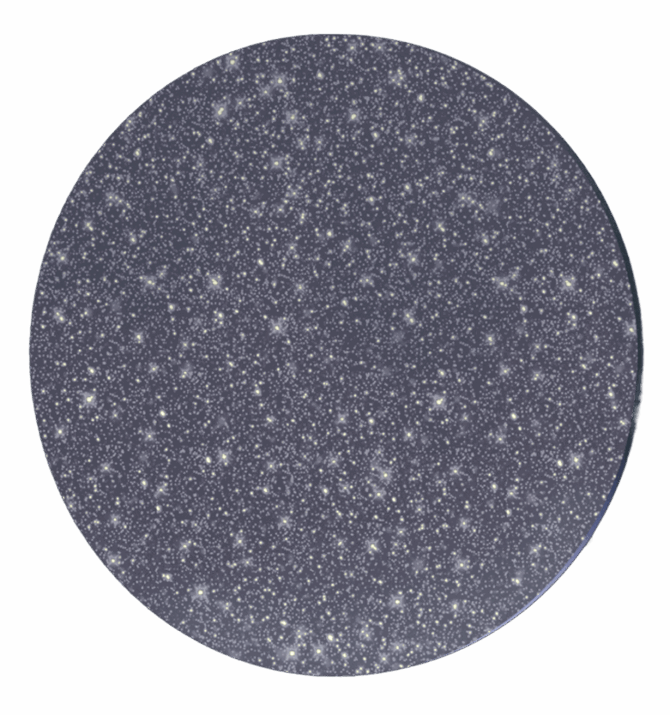
Single Poly crystal diamond wafer
What are Single-Crystal Diamond Wafer?
Single crystal diamond wafer are highly advanced, lab-grown semiconductor substrates crafted from pure, single-crystalline diamond material. Unlike natural diamonds, which contain imperfections and variable properties, lab-grown single crystal diamond wafers are engineered for flawless consistency and exceptional electronic-grade quality.
These wafers represent a breakthrough technology in the semiconductor industry due to their unmatched combination of properties, including:
Exceptional Thermal Conductivity
Diamond wafers boast thermal conductivity exceeding 2,200 W/m·K, making them the ultimate material for heat dissipation in high-performance electronics.
Ultra-Wide Bandgap Material
With a bandgap of 5.47 eV, diamond wafers operate efficiently at extremely high voltages, frequencies, and temperatures, surpassing silicon (Si), silicon carbide (SiC), and gallium nitride (GaN).
High Breakdown Voltage
Diamond wafers can sustain electrical fields greater than 10 MV/cm, enabling devices to handle higher voltages and power levels without breakdown.
Superior Stability & Reliability
Chemically inert and extremely hard, diamond wafers provide unparalleled durability and longevity, ideal for harsh environments and mission-critical applications.

Polycrystalline Diamond Wafers
What are Polycrystalline Diamond Wafers?
Polycrystalline diamond wafers (often abbreviated as PCD wafers) are advanced, lab-grown diamond substrates made from numerous microscopic diamond crystals fused seamlessly together. Unlike single crystal diamond wafers, polycrystalline wafers have multiple crystal grains arranged randomly, providing exceptional versatility and durability at a more accessible price point.
High Thermal Conductivity
Polycrystalline diamond wafers offer thermal conductivity ranging from 1,200 to 1,800 W/m·K, significantly outperforming silicon (Si), silicon carbide (SiC), and gallium nitride (GaN), making them excellent for thermal management in electronics.
Extreme Hardness and Wear Resistance
Renowned for their durability, polycrystalline diamond wafers excel in applications that require high wear resistance, abrasion resistance, and toughness, extending product life and reliability.
Electrical Insulation
With excellent dielectric properties, these wafers are ideal substrates for electrically insulating and thermally conductive applications
Cost-Effectiveness and Scalability
Polycrystalline wafers provide many advantages of diamond at a lower cost and are easier to produce at larger sizes, enhancing commercial viability and scalability.

Which One to Choose?
If you need ultra-high thermal conductivity, electronic performance, or quantum applications, SCD wafers are the best choice. f you need large-scale thermal management, industrial durability, or cost-effective solutions, PCD wafers are more practical.
| Feature | Single-Crystal Diamond (SCD) Wafers | Polycrystalline Diamond (PCD) Wafers |
|---|---|---|
| Crystal Structure | A continuous, defect-free lattice of carbon atoms. | Composed of many small diamond grains with grain boundaries. |
| Thermal Conductivity | Extremely high (~2200 W/m-K for pure SCD). | Slightly lower (~1000-2000 W/m.K due to grain boundaries). |
| Electrical Properties | Naturally an electrical insulator but can be doped for semiconductors. | Typically an insulator, but grain boundaries can affect conductivity. |
| Mechanical Strength | Higher purity and structural integrity. | Slightly less strong due to grain boundaries. |
| Optical Transparency | Extremely clear and transparent to a broad range of wavelengths. | Less transparent due to grain boundaries causing light scattering. |
| Manufacturing Complexity | Difficult and expensive to grow via CVD (Chemical Vapor Deposition). | Easier and cheaper to produce, grown over a larger area. |
| Size Availability | Limited to smaller sizes (~10-20 mm) due to growth constraints. | Can be grown in larger wafer sizes (50 mm+). |
| Cost | More expensive due to complex fabrication and purity. | More cost-effective for large-scale applications. |
Single crystal diamond wafers
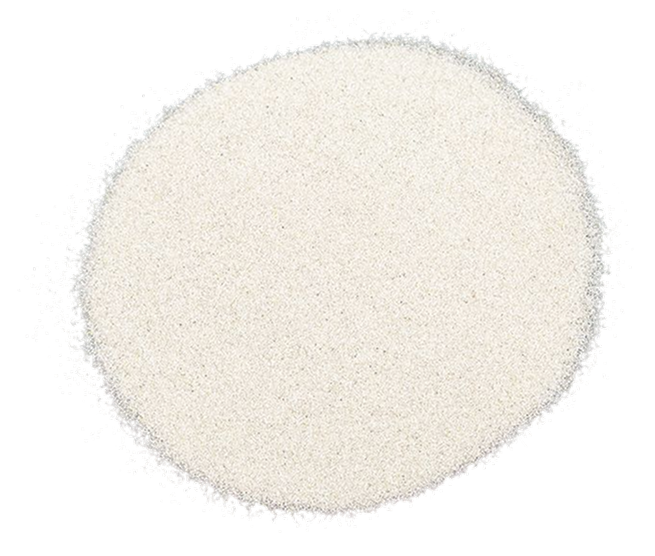
What are Diamond Powders?
Diamond powders are finely-ground, precision-engineered particles of diamond, typically produced from synthetic, lab-grown diamond crystals. Known for their extreme hardness, exceptional thermal conductivity, and chemical stability, diamond powders serve as the ideal abrasive and functional additive across diverse industries.
Key Characteristics and Benefits:
Superior Hardness & Abrasion Resistance
Diamond powders provide unmatched abrasive performance for precision polishing, grinding, and cutting operations.
Exceptional Thermal Conductivity
Their outstanding heat transfer capability enhances cooling efficiency, beneficial in electronics and thermal management applications.
Chemical Stability & Durability
Resistant to chemicals and high temperatures, diamond powders ensure reliability in demanding environments.
Controlled Particle Sizes & Shapes
Available in precise sizes from nanometers to microns, enabling optimized performance for specific applications.
| Parameters | Diamond Powder (Industrial) | Silicon Carbide (SiC) | Aluminum Oxide (AI2O3) | Cubin Boron Nitride (CBN) |
|---|---|---|---|---|
| Hardness (Mohs scale) | 10 (highest known) | 9.9 - 5 | ~9 | 9.5 (second hardest after diamond) |
| Thermal Conductivity | 900-2200 W/m.K | ~490 W/m.K | 30-40 W/m.K | ~740 W/m.K |
| Typical Particle Size | 0.1-500 μm (highly customizable) | 1-500 μm | 1-500 μm | 1-500 μm |
| Wear Resistance | Exceptional (highest) | Excellent | Very Good | Excellent |
| Chemical Stability | High (resistant to most acids and bases) | Very High (stable, chemically inert) | High (good chemical resistance) | Extremely High (superior thermal and chemical stability) |
| Thermal Stability | Up to ~700°C | >1600°C | ~1500°C | >1200°C |
| Cost per kg | $400-$2,000+ | $5-$30 | $2-$10 | $2,000-$7,000+ (typical) |